SC Solutions develops physics-based models of chambers for Metal-Organic Chemical Vapor Deposition (MOCVD). Our capability is illustrated here using an example from the literature (U.S. Patent 8778079).
BACKGROUND
MOCVD is a deposition technique used to grow thin films on solid substrates (wafers) using organo-metallic compounds as sources. The films grown by MOCVD are usually semiconductors and are primarily used for the fabrication of electronic and optoelectronic devices that are components of cell phones , optical communication, optical storage, light emitting diodes (LEDs), and solar cells. MOCVD is used to build up multiple layers of different materials, each of a precisely controlled thickness, to engineer a material with desired optical and electrical properties.
FEM MODEL OF CHAMBER
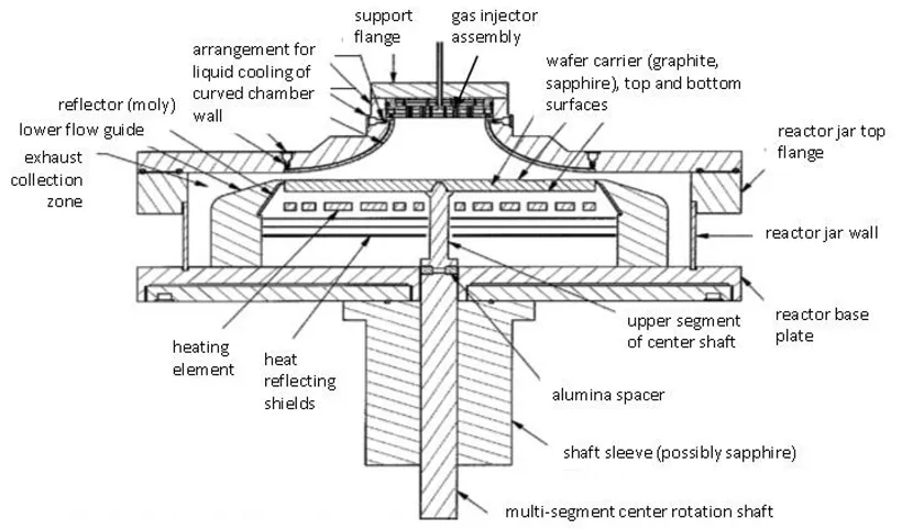
SC built a FEM model of the chamber described in U.S. Patent 8778079 using COMSOL software. FIGURE 1 shows a cross sectional view of the chamber and other components. A two-dimensional (2D) axisymmetric FEM model of the chamber with a rotating susceptor was developed. The model incorporates gas flow, and conduction and radiation heat transfer throughout the chamber. The gas below the susceptor is nitrogen while the gas in the chamber above the susceptor is hydrogen. The six tungsten heaters below the susceptor are connected to three power supplies, with middle four heaters grouped together.
A two-dimensional (2D) axisymmetric FEM model of the chamber with a rotating susceptor was developed. The model incorporates gas flow, and conduction and radiation heat transfer throughout the chamber. The gas below the susceptor is nitrogen while the gas in the chamber above the susceptor is hydrogen. The six tungsten heaters below the susceptor are connected to three power supplies, with middle four heaters grouped together.